TOKYO
,
February 21, 2023
(press release)
–
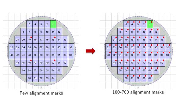
Canon Inc. announced today the launch in Japan of the MS-001, a high-precision wafer alignment1 measurement device for semiconductor lithography systems. MS-001 Additional alignment marks (conceptual image) In the manufacturing process of advanced semiconductors including logic and memory chips, the deformation of wafers is increasingly becoming an issue due to the growing complexity of the manufacturing process. To manufacture semiconductor devices, wafer deformation must be measured accurately in order to overlay and expose with high precision multiple layers of circuit patterns within a series of lithography systems. To ensure the high accuracy required for overlay, alignment marks on wafers have increased from fewer points in the past to hundreds in modern processes. Therefore, measuring hundreds of alignment marks results in significant time cost, thus reducing the productivity of the lithography systems. The MS-001 allows the majority of alignment measurements to be performed in one batch process—outside the lithography system, before it receives the wafer—thus improving the productivity of the lithography system by reducing the number of measurements performed inside them. Canon's MS-001, equipped with an alignment scope that adopts an area sensor for multiple-pixel, low-noise imaging can measure even low-contrast alignment marks, making possible measurement of more types of alignment marks than can be measured by conventional lithography systems. In addition, a newly developed light source for the alignment scope enables MS-001 to use 1.5 times the wavelength range of measurements2, giving users more freedom in selecting wavelength bands for measurement. Thus, MS-001 can measure alignment marks with higher accuracy than conventional semiconductor lithography systems. Together with Canon's Lithography Plus solution (released in September 2022), users can aggregate operating status information from semiconductor lithography systems with data from the MS-001. By cross-referencing and monitoring MS-001 measurement data with other collected information using Lithography Plus, changes to the on-wafer alignment information can be detected, allowing automatic correction by the semiconductor lithography system. Utilizing Canon's Lithography Plus solution, MS-001 also enables system owners to achieve centralized control of the alignment measurement and exposure processes, resulting in a reduced cost of ownership (CoO3).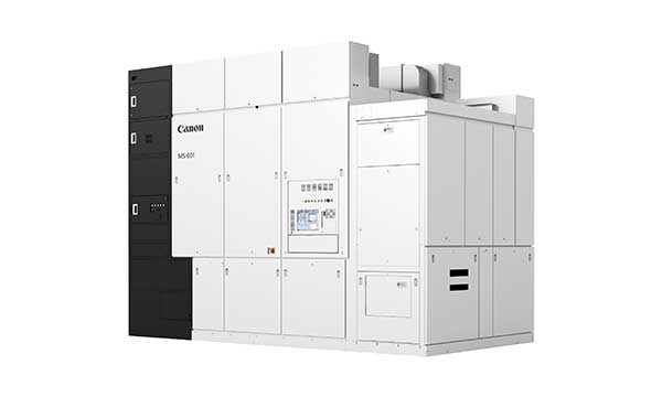
Related Links
* All content is copyrighted by Industry Intelligence, or the original respective author or source. You may not recirculate, redistrubte or publish the analysis and presentation included in the service without Industry Intelligence's prior written consent. Please review our terms of use.


