TOKYO
,
March 13, 2023
(press release)
–
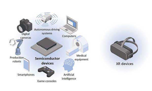
Canon Inc. announced today that the company will release the FPA-5550iX i-line stepper1 semiconductor lithography system for front-end processes that realizes a large exposure field of 50 x 50 mm and a high resolution of 0.5 micrometers2. FPA-5550iX Production of diverse range of devices The new system features a large exposure field of 50 x 50 mm and a high resolution of 0.5 micrometers making possible single exposure of a large field with the high resolution required to produce full-frame CMOS sensors and other devices in which higher precision is advancing. The new system is also capable of manufacturing small displays for such devices as head-mounted displays. It also enables the high-resolution single exposure required for manufacturing high-contrast micro-OLED panels3 with wide viewing angles, which are expected to grow as displays for cutting-edge XR devices. In addition to semiconductor devices, the new FPA-5550iX can also manufacture displays for cutting-edge XR devices, thus supporting the manufacture of a wide range of devices. The FPA-5550iX utilizes the same projection lens used by its predecessor model, the FPA-5510iX (released in September 2015) which enables a high resolution of 0.5µm. Thanks to a wide exposure field of 50 x 50 mm, the system can perform high-resolution single exposure for full-frame CMOS sensors, next-generation displays for XR devices and more. What's more, manufacturing processes have been refined to ensure high-quality, stable production of projection lenses, many of which are used in the system, to meet the strong demand expected for semiconductor lithography systems. In addition, a new alignment scope that can read wider variety of alignment marks4 has expanded the range of processes in which FPA-5550iX can be used. In addition to the "bright-field detection" function for measuring direct light, a new "dark-field detection" function has been added to the alignment scope, enabling the measuring of scattered and diffracted light, thus allowing users to select a wide range of measurement methods. Low-noise measurement has been made possible by expanding the range of usable wavelengths while also employing an area sensor for multi-pixel measurement. Thanks to these advancements, the system can detect and measure low-contrast alignment marks. What's more, the system can optionally select an infrared wavelength that can pass through silicon, enabling users to measure the alignment on the back of the wafer, which is a requirement for the manufacture of back-illuminated sensors. The flexibility of alignment mark measurement thus allows the system to be utilized in a variety of processes. When combined with Canon's Lithography Plus solution platform (released in September 2022), the FPA-5550iX, provides operators with the ability to monitor the condition of the lithography system, as well as perform analyses, helping them maintain appropriate quality control and higher utilization rates.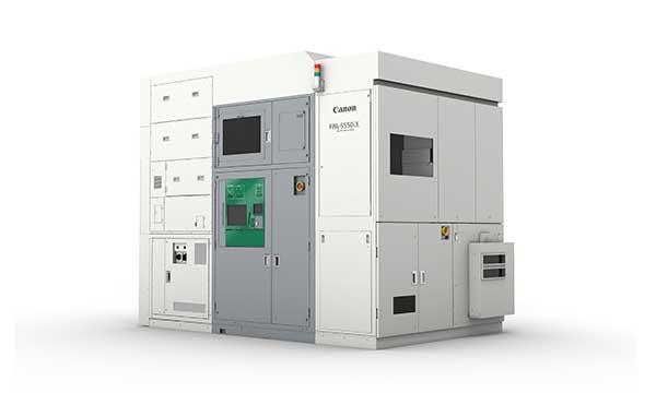
* All content is copyrighted by Industry Intelligence, or the original respective author or source. You may not recirculate, redistrubte or publish the analysis and presentation included in the service without Industry Intelligence's prior written consent. Please review our terms of use.
